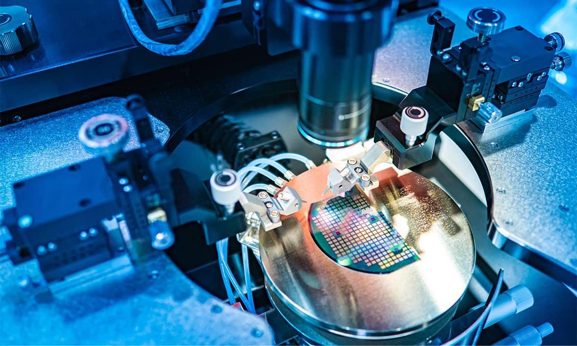


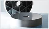


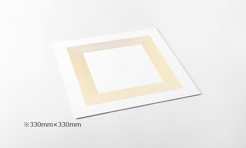
Metallized Large Ceramic Substrate
Kyocera's ceramic metallization technology achieves larger component sizes, high positional accuracy by leveraging large substrate forming technology, and high-precision post-firing laser processing and patterning. Additionally, we offer a wide range of pattern materials such as Ag, Cu, Pt, glass, and resistors, allowing you to select the optimal material according to your needs.
Features
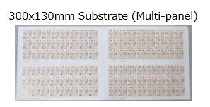
- Larger Size
Compatible with large substrates up to 330mm square. *Please inquire for even larger sizes. - Wide range of materials
From ceramic materials such as alumina, silicon nitride, and aluminum nitride, to pattern materials like Cu, Ag, and Pt, and even plating materials, you can select the optimal material for your application. - High Positional Accuracy
・Laser Processing: Supports scribe (dicing groove) processing, Via hole processing (>Φ0.1mm), and through-hole processing.
・Laser Processing Accuracy: 330±0.05mm
・Pattern Positional Accuracy: 330±0.15mm
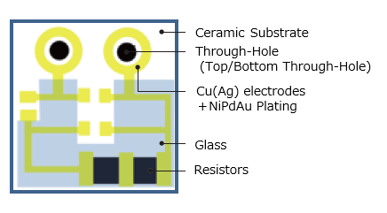
Basic Structure
Shows basic structure, standard thickness/specifications.
・Cu or Ag + Glass + NiPdAu Plating
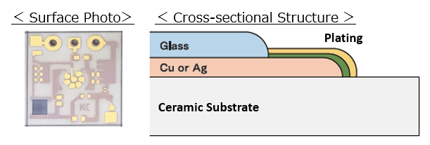
| Item | Material | Standard Thickness / Specifications | |
|---|---|---|---|
| Electrode Materials | Cu/Ag | >10μm | |
| Plating Materials | Electroless Ni-Pd-Au |
Ni | 1.27~8.89μm |
| Pd | 0.10~0.50μm | ||
| Au | 0.05~0.15μm | ||
| Resistive Materials | Resistance | Rs=0.6~3000Ω (Outside the range can also be considered) | |
| Protective Film Materials | Glass | >10μm | |
| Resin | >10μm | ||
*Please consult for anything outside the above range.
Material Lineup
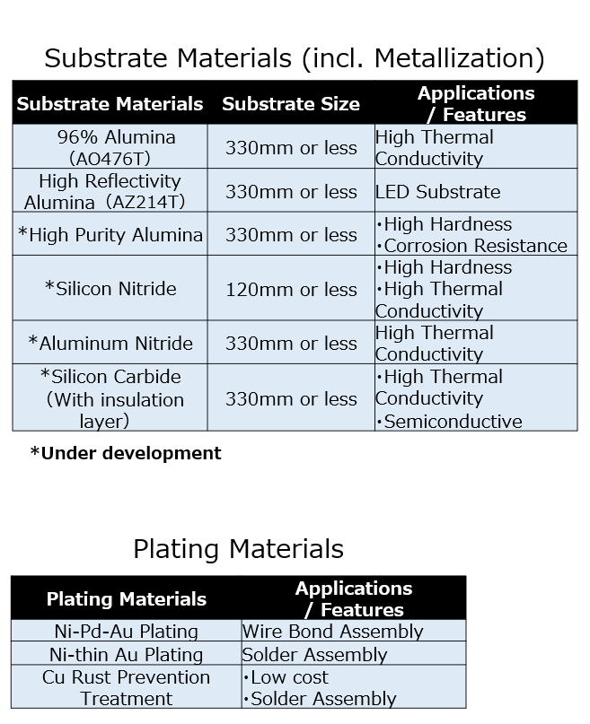
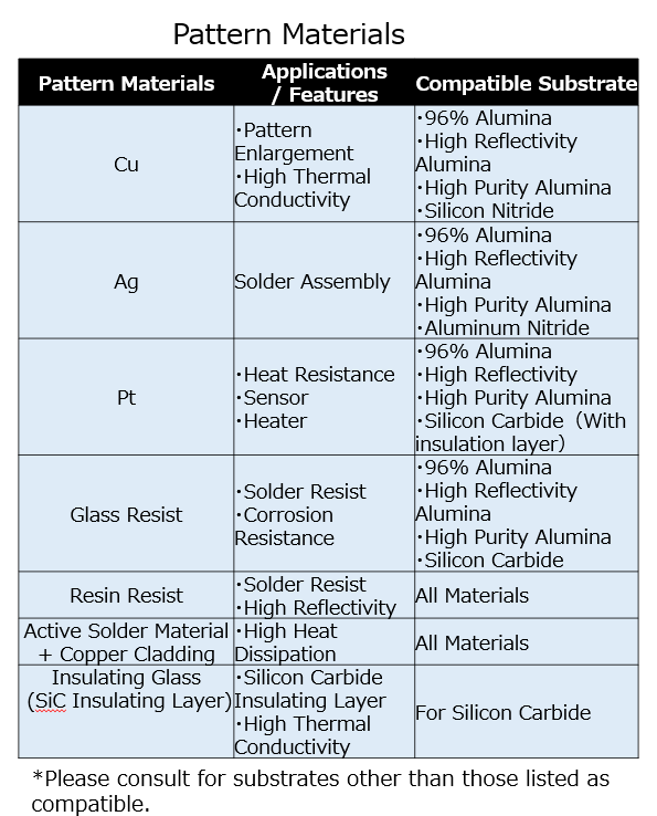
*For ceramic material characteristics + electrode material variations and various combinations, please consult us.
Feature Details
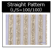
Larger Size / High Positional Accuracy
・Larger Size: Compatible with large substrates up to 330mm square.*Please inquire for even larger sizes.
・Laser Processing Accuracy: 330±0.05mm
・Pattern Positional Accuracy: 330±0.15mm
・Fine Patterning: Current L/S=200μm (100μm under development)
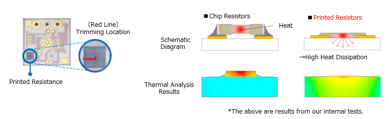
Printed Resistance / Trimming
By adopting printed resistors, the following advantages can be obtained compared to chip resistors.
・Improved mounting area efficiency and design flexibility due to reduced number of components.
・High-precision resistance value adjustment through laser trimming (Adjustment tolerance: ±2%).
・Functional trimming allows for resistance optimization per component.
・Ensures high heat dissipation with a printed structure, achieving improved rated power.
*Please consult regarding the trimming processing range, as there are limitations.
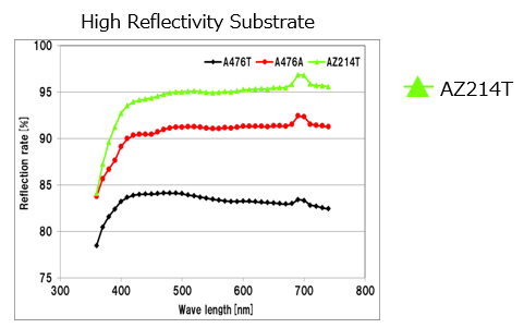
High Reflectivity
We also offer materials with high reflectivity as substrate materials.
・High Reflectivity Alumina Substrate (AZ214T)
(Reflectivity: 95%)
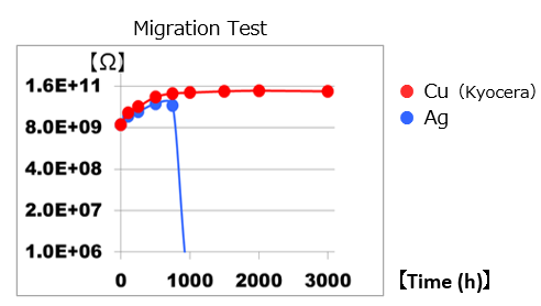
Migration Resistance
It is possible to select Cu electrodes with excellent migration resistance. (UL certification acquired)
Application Examples
LED Applications (Automotive, General Lighting)
・LED Substrate (Rear / Brake / Winker)
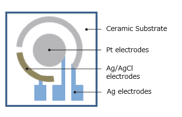
Sensor Substrate
・Bio-sensors, etc.
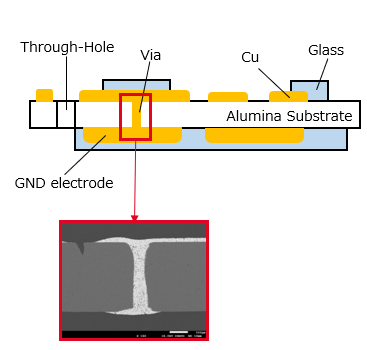
Top and Bottom Via (Φ0.1~0.4)
Circuit formation including the back side is also possible.
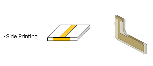
3D Shape
Electrode printing is possible on the ceramic substrate sides, cylindrical outer surfaces, and curved surfaces.
All values listed on this page are representative values obtained from in-house measurements,
and do not constitute guaranteed product specifications.